Photovoltaic Technologies
Due production technology used solar cells can be divided into silicon solar cells, produced from Si wafers, and thin-film solar cells produced with vacuum technologies. According to the crystalline structure amorphous, poly-crystalline and mono-crystalline solar cells are distinguished. Solar cells are connected together and many solar cells represent a solar module with typical power range of up to two houndred watts or even more. For large PV systems special PV modules are produced with typical power range of up to several houndred watts. The solar module properties depend mainly on the solar cell type used. The most important tasks in the future are utilisation of less pure silicon and increasing efficiency (monocrystalline solar cells) and increasing efficiency and life-time (amorphous solar cells).
Silicon, Basic Features
The most important material for solar cells production is silicon. At the time being it is almost the only material used for solar cell mass production. As the most often used semiconductor material it has many important advantages. In nature it can be easily found in large quantities. Silicon oxide forms one thirth of the Earth's crust. It is not poisonous, and it is environment friendly, its waste does not represent any problems. It can be easily melted, handled, and it is fairly easy formed into mono-crystalline form. Its electrical properties with endurance of 125°C allow the use of silicon semiconductor devices even in the most harsh environment and applications. In technics, pure silicon is the only widely used chemical element produced so pure. The percentage of pure silicon in material is at least 99.9999999 %. According to density of silicon, which is 5⋅1022 atoms/cm3, it means 5⋅1013 impure atoms/cm3. Impure atoms values are investigated due to numerous specific physical methods like mass spectrometry and similar sophisticated measurements. Pure silicon is produced from sand (SiO2). In production the following procedure below described processes are performed.
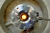
Silicon crystaline structure and pure raw silicone
(courtesy: Helmholtz-Zentrum,
SolarWorld)
Production of raw silicon
Pure silicon is produced from silicon by reduction in specially designed furnaces at 1800°C. The produced material contains 98-99 % of pure silicon. As a reducer carbon electrodes are used. The complete reaction is as follows:
SiO2 + C → Si + CO2
Such silicon is used as raw material in production of pure silicon. It is also used in steel and aluminium production procedures as a supplement material. The most important producers of raw silicon are Canada, Norway and Brazil. 15 to 25 kWh of electrical energy is needed to produce a kg of silicon. Silicon tetra-chloride (gas) is produced by chlorination of fine ground metallurgic silicon in special reactor. Additions or impurities are eliminated in the form of chlorine salt.
Si + 2Cl → SiCl4
The following reactions result in tri-chlorine-silan gas:
SiCl2 + HCl → SiHCl3
The gas is then additionally purified, removing any remaining tetra-chlorine-silan and other silans. The purifying is followed by reduction in hydrogen atmosphere at 950°C:
4SiHCl3 + H2 → 2Si + SiCl4 + SiCl2 +6HCl
Besides pure silicon the procedure results in a number of side products. Their origin is gaseous and they condense outside of the reactor. The presented example depicts one possible way of producing pure silicon. There are other production procedures with different chemical reactions used, yet the end product is the same - pure silicon.


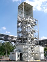
Reactor for producing raw silicone and silicon crystalisation process
(courtesy: SolarWorld)
Polycrystalline Silicon Production
The procedure of extracting pure poly-crystalline silicon from tri-chlorine-silan can be (among others) performed in special furnaces developed by Siemens. Furnaces are heated by electric current, which flows through (in most cases) silicon electrodes. 2 m long electrodes measure 8 mm in diameter. The current flowing through electrodes can reach up to 6000 A. The furnace walls are additionally cooled preventing formation of any unwanted reactions due to gas side products. The procedure results in pure poly-crystalline silicon used as a raw material for solar cell production. Poly-crystalline silicon can be extracted from silicon by heating it up to 1500°C and then cooling it down to 1412°C, which is just above solidification of the material. The cooling is accompanied by origination of an ingot of fibrous-structured poly-crystalline silicon of dimensions 40x40x30 cm. The structure of poly-crystalline silicon in part of the material is settled, yet it is not adjusted to the structure of the other part.
Monocrystalline Silicon
Two different technological procedures are used to produced mono-crystalline silicon from pure silicon:
By utilization of Czochralski method [1], silicon is extracted from melt in induction oven with graphite lining at the temperature of 1415°C. Silicon crystal of defined orientation is placed on a rod. In the melt, spinning the rod makes the crystal grow. The rod spinning speed comes to 10 to 40 turns per minute, whilst the movement at length comes between 1 μm and 1 mm per second. It allows production of rods, which measure 30 cm in diameter and several metres in length. It all takes place in inert atmosphere. Possible impurities burn or eliminate in the melt.
Using float zone monocrystalline silicon is produced from polycrystalline silicon. The main advantage of this procedure is higher pure silicon production. The silicon rods produced Silicon rod measure 1 m in length and 10 cm in diameter. The procedure, where induction heater travels along the rod melting silicon, also takes place in inert atmosphere. Mono crystal silicon originates from the cooling. Monocrystalline or polycrystalline silicon ingots are then sawn and the wafers are worked upon until they can serve as foundation for solar cell production. By sawing approximately 50 % of material is wasted.
Amorphous Silicon
Amorphous silicon is produced in high frequency furnaces in partial vacuum atmosphere. At presence of high frequency electrical field, gases like silan, B2H6 or PH3 are blown through the furnaces supplying silicon with boron and phosphorus.
Galium-Arsenide (GaAs)
GaAs is used for production of high efficiency solar cells. It is often utilized in concentrated PV systems and space applications. Their efficiency is up to 25 %, and up to 28 % at concentrated solar radiation. Special types have efficiency over 30 %.
Cadmium-Telluride (CdTe)
Thin-film material produced by deposition or by sputtering is a promising low cost foundation for photovoltaic applications in the future. The procedure disadvantage is poisonous material used in production. Lab solar cells efficiency is up to 16 %, whilst the commercial types efficiency is up to 8 %.
Copper-Indium-Diselenide (CuInSe2, CIS)
Thin-film material with efficiency of up to 17 %. The material is promising, yet not widely used due to production specific procedures.
Crystalline silicon solar cells
Polycrystalline as well as monocrystalline solar cells belong into this group. The basic form for crystalline solar cells production is silicon ingot (please see production procedure description above). The ingot (block of silicon), sawn with diamond saw into thin silicon wafers, is a foundation for solar cell production. Wafers of 1 mm in thickness sawn with 1/10 mm precision are placed between two plan-parallel metal plates, which rotate into opposite directions. The procedure enables wafer thickness adjustment to 1/1000 mm precisely.


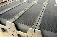
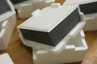
Silicon before sawing, sawed wafers and wafers ready for delivery
(courtesy: SolarWorld)
Doped wafers are first etched some micro-metres deep. The procedure removes crystal-structure irregularities caused by sawing and provides wafer cleaning. The material is doped as melt at polycrystal silicon or adequate gas is added whilst extracting pure silicon. The above procedure is followed by diffusion. Phosphorus, which is supplied inside the material in gaseous form, diffuses at the temperature of 800 °C. N doped layer and oxide layer rich with phosphorus form on top of wafers due to oxygen reaction. Wafers are then folded to form a cube and etched in oxygen plasma, removing N layer from the edges. The following phase removes oxide layers from top of wafer by wet chemical etching. In the back, contact surface is produced from silver containing 1 % aluminium. Special procedures enable silver print over mask on cell surface. Pressed cells are then sintered at high temperatures. Similar procedure is used to print contacts in the front cell surface. Anti-reflex layer is applied in a similar manner. We have titanium paste at choice, which at sintering form titanium dioxide TiO2 or silicon nitride Si3N4.
Notes
| [1] | Czochralski method is named by polish scientist Jan Czochralski who invented it. More about history of photovoltaics is available in history section. |
Organic Solar Cells
Linz Institute for Organic Solar Cells (LIOS) - Institute of Physical Chemistry.
Petritsch, K.: Organic Solar Cell Architecture, PhD Thesis, Cambridge 2000.
Other Technologies
NanoFlex Power - flexible organic solar cells.
sphelar power - spherical solar cells technology.

